
Audio D/A Converters
-
[Q0022]
・Tell me power-down release (power up) sequence after tuning power supplies on.
-
A.
・Turn power supplies on while the PDN pin = "L" and then set the PDN pin to "H" after Reset period (tPD) is passed.
Was it helpful?YesNoThank you We will reflect your opinion on the improvement of the web content.
-
[Q0023]
・Tell me clock input timing at start-up.
-
A.
・A clock can be input anytime after power supplies are turned on. However, if the clock is input after releasing power-down, internal circuit timing starts by a clock input and then the analog block is powered up.
Was it helpful?YesNoThank you We will reflect your opinion on the improvement of the web content.
-
[Q0024]
・If the device supports clock power-down mode, what is the analog output pin's status in power-down mode when MCLK and LRCK are stopped?
-
A.
・The analog out pins are in Hi-Z state.
Was it helpful?YesNoThank you We will reflect your opinion on the improvement of the web content.
-
[Q0025]
・If the device supports clock power-down, will register settings be cleared and become default value by clock power-down?
-
A.
・Register settings will not be initialized by clock power down.
Was it helpful?YesNoThank you We will reflect your opinion on the improvement of the web content.
-
[Q0026]
・What should be the master clock frequency when using TDM256 mode with 44.1kHz sampling frequency?
-
A.
・Input a master clock that is equal or faster than 11.2896MHz (256fs). Please refer to the datasheet of each device in detail.
Was it helpful?YesNoThank you We will reflect your opinion on the improvement of the web content.
-
[Q0027]
・Are there any specifications of overshoot and undershoot in the digital input signal?
-
A.
・Overshoot and undershoot of digital inputs are not specified. Operation beyond VIND limits may result in permanent damage to the device. Normal operation is not guaranteed at this extreme.
Was it helpful?YesNoThank you We will reflect your opinion on the improvement of the web content.
-
[Q0028]
・How much capacitance does the digital input pin have?
-
A.
・The input capacitance will be less than 5pF.
Was it helpful?YesNoThank you We will reflect your opinion on the improvement of the web content.
-
[Q0029]
・How should the unused analog output pins be handled?
-
A.
・They should be handled as open.
Was it helpful?YesNoThank you We will reflect your opinion on the improvement of the web content.
-
[Q0030]
・What is the output resistance value of the analog output pin?
-
A.
・Output resistance value is not being specified and guaranteed. It will be 1Ω or less as the actual value.
Was it helpful?YesNoThank you We will reflect your opinion on the improvement of the web content.
-
[Q0031]
・What are advantages and disadvantages when the capacitance connected to the VCOM pin becomes smaller?
-
A.
・Advantage: The startup time is faster than normal.
 Disadvantage:
 1 - It is more susceptible to noise influence. SNR performance may be degraded.
 2 - Transient of "pop" noise shall be increased upon power up.
Was it helpful?YesNoThank you We will reflect your opinion on the improvement of the web content.
-
[Q0032]
・What happens to the analog output if digital data is input before the the VCOM voltage is stable?
-
A.
・Please note that the analog output waveform may be distorted if digital data in input before the VCOM voltage is stable.
Was it helpful?YesNoThank you We will reflect your opinion on the improvement of the web content.
-
[Q0033]
・Regarding the Load Resistance of dac what input frequency do this product specify? The condition of input frequency is only 1kHz?
-
A.
・Input signal frequency is specified from 20Hz to 20kHz. It obtains a load that can drive an amplifier at the following stage.
Was it helpful?YesNoThank you We will reflect your opinion on the improvement of the web content.
-
[Q0034]
・Does the DAC generate stable DC output ?
-
A.
・The DAC can generate a DC output. However, there are no tested and guaranteed performance/accuracy specs below the range of 20Hz to 20kHz.
Was it helpful?YesNoThank you We will reflect your opinion on the improvement of the web content.
-
[Q0035]
・Do you have a circuit diagram of external analog filter that converts differential output to single-ended signal and the calculation formula of frequency characteristics?
-
A.
・The circuit diagram of external analog filter and LPF calculation formula are written in Analog Output of the datasheet and the evaluation board manual. (example AK4482)
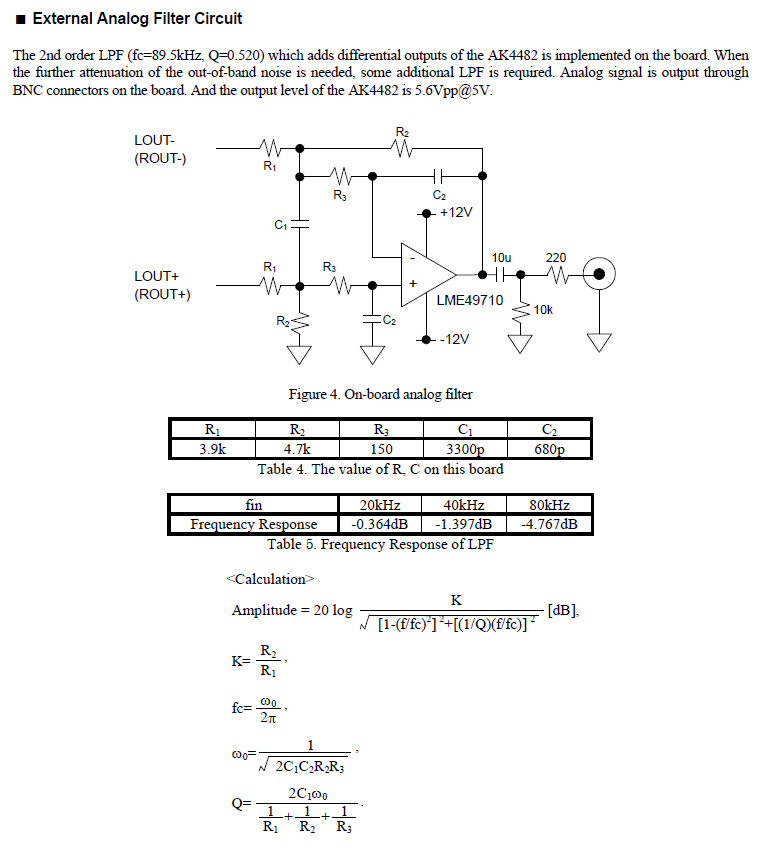
External Analog Filter Circuit Was it helpful?YesNoThank you We will reflect your opinion on the improvement of the web content.
-
[Q0036]
・What is the definition of Group Delay? Is there any reason for that they don't have min/max values?
-
A.
・The definition of the group delay is the time from data coming in the device to data output to the device at their respective pins. This usually shows in number of 1/fs unit.This is mainly caused by the taps of the digital filter. Therefore there are no variations.
Was it helpful?YesNoThank you We will reflect your opinion on the improvement of the web content.
-
[Q0037]
・Is there phase difference between channels if the device has multiple input channels?
-
A.
・There is no phase difference between channels.
Was it helpful?YesNoThank you We will reflect your opinion on the improvement of the web content.
-
[Q0038]
・Is a wait time necessary to start accessing to registers after releasing power-down (PDN pin: "L"→ "H") ?
-
A.
・A wait time is not necessary since register access is available after power-down is released.
Was it helpful?YesNoThank you We will reflect your opinion on the improvement of the web content.
-
[Q0039]
・What happens to written data if the data communication from HOST is cut forcibly by setting the CSN pin to "H" ?
-
A.
・Written commands are cancelled and registers are not updated if the CSN pin is set to "H" from "L" during a communication.
Was it helpful?YesNoThank you We will reflect your opinion on the improvement of the web content.
-
[Q0040]
・Do you have the register setting and the external post circuit block in the mono mode?
-
A.
・A circuit schematic diagram is shown here (AK4490).
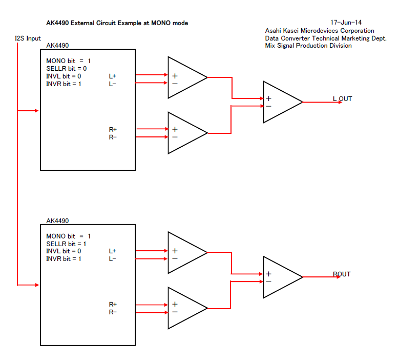
AK4490 External Circuit Example Was it helpful?YesNoThank you We will reflect your opinion on the improvement of the web content.